TI官方例程中,为了保证应用层的扩展性,做了多重函数封装,根据上一篇文章《深入CC3200(4)—GPIO相关函数解析(1)》,通过GPIOPinWrite()函数可以设置GPIO的电平高低,比如:
//前面说过GPIO对应PA1口第1 BIT位(10b)即:GPIO9,输出值为0
GPIOPinWrite(GPIOA1_BASE, 0x02, 0 << 1);
注:接下来就此函数进行详细分析。
1. 查看GPIOPinWrite函数内部的具体实现,如下:
void GPIOPinWrite(unsigned long ulPort, unsigned char ucPins, unsigned char ucVal);
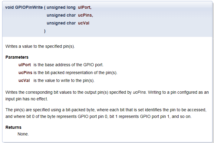
void GPIOPinWrite(unsigned long ulPort, unsigned char ucPins, unsigned char ucVal)
{
    //监测输入的值是否合法
    ASSERT(GPIOBaseValid(ulPort));

    //设置某地址所对应寄存器的值
    HWREG(ulPort + (GPIO_O_GPIO_DATA + (ucPins << 2))) = ucVal;
}
其中,HWREG函数可以在目录:C:\TI\CC3200SDK_1.1.0\cc3200-sdk\inc 下hw_types.h中找到,定义如下:
#define HWREG(x) (*((volatile unsigned long *)(x)))
综上,最终即实现对地址为X的寄存器设置值ucVal。
2.****接下来计算HWREG函数中的寄存器地址:
其定义可查看文件hw_gpio.h和hw_memmap.h,计算结果如下:
ulPort + (GPIO_O_GPIO_DATA + (ucPins << 2)) = GPIOA1_BASE+(0x00000000+0x02<<2)
                        = 0x40005000+0x02<<2 = 0x40005000+0x08
                        = 0x40005008
3. 分析上面值代表的含义:
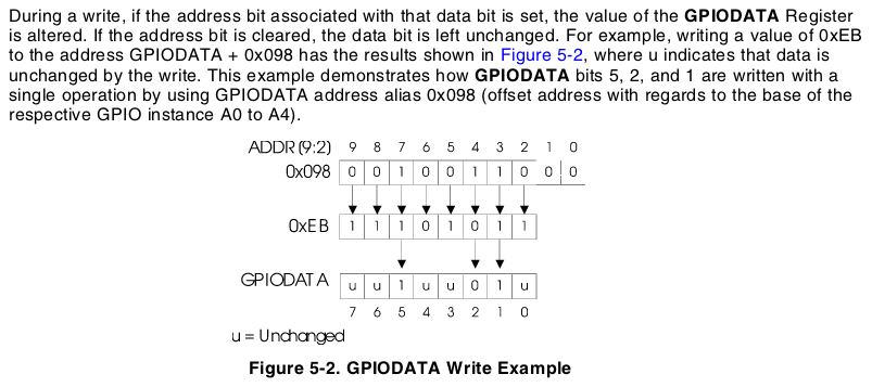
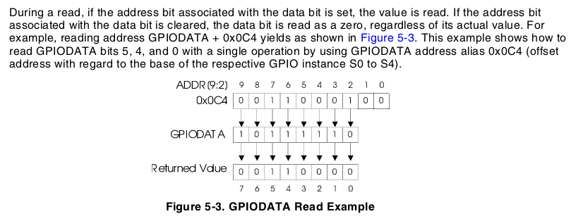
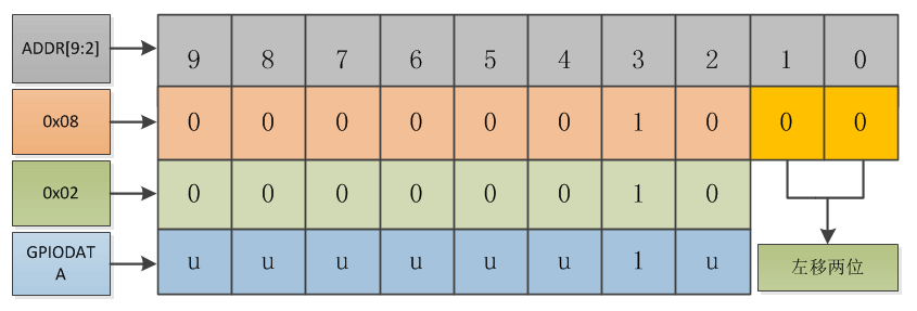
根据编程手册P116知,在CC3200数据寄存器操作时,读写数据寄存器被地址[9:2]位所屏蔽,即设置相应的数据时,其数据和地址[9:2]位做一定运算,此处的ucPins需要左移2位,解释如下:
To facilitate the reading and writing of data to these registers by independent drivers, the data read from and written to the registers are masked by the eight address lines [9:2].
Reads from this register return its current state.
Writes to this register only affect bits that are not masked by ADDR[9:2] and are configured as outputs.
详细过程如下:
4. GPIO寄存器内容运算方法如上所述,以****GPIOPinWrite设置GPIO9为例:
GPIOPinWrite(GPIOA1_BASE, 0x02, 0 << 1);   //GPIO9
MAP_UtilsDelay(8000000);   //延迟
GPIOPinWrite(GPIOA1_BASE, 0x02, 1 << 1);   //GPIO9
MAP_UtilsDelay(8000000);
具体实现过程如下图所示:
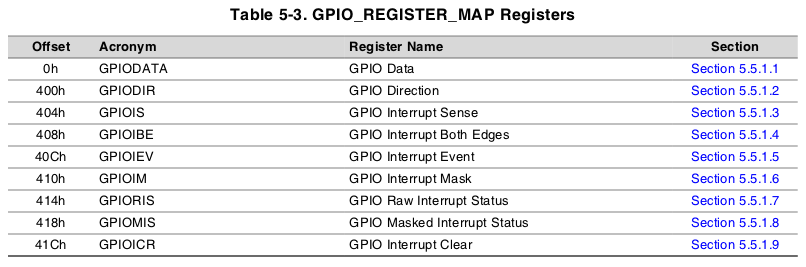
5. 附GPIO相关的寄存器,如下: